Spice Simulation of (not only) Silicon Photomultipliers and Design of a small sized Scintillation Detection Unit
The idea behind this post is to show you how I build a basic detection unit for ionizing radiation which i then used to derive a spice model from it. The spice model shell then be used to develop additional electronics for further investigation of the detected ionizing radiation.
But before going into topic, let’s get some basics first.
Plastic Scintillators
Scintillators are materials that emit light when hit by ionizing radiation or high energy particles. Plastic scintillators are scintillators in which the primary fluorescent emitter is a polymer. The light emitted by this primary emitter is most likely in the UV range has to be shifted in it’s spectrum by a secondary fluorescent emitter to not be directly absorbed again. The light attenuation length is a property that’s often given in the datasheet of scintillators. It’s the distance a photon of a certain wavelength $\lambda$ has travelled inside the scintillator at which the probability to find this photon there has dropped to $\frac{1}{e}$.
$$ \begin{eqnarray} P(x) &=& e^{\frac{-x}{\lambda}} \newline \frac{1}{e} &=& e^{\frac{- \text{light attenuation length}}{\lambda}} \end{eqnarray} $$
The advantage of plastic scintillators is that they have a fairly high light output, a low decay time of $2$ to $4~ns$, they do not cost much and can be shaped easily.
Silicon Photomultipliers
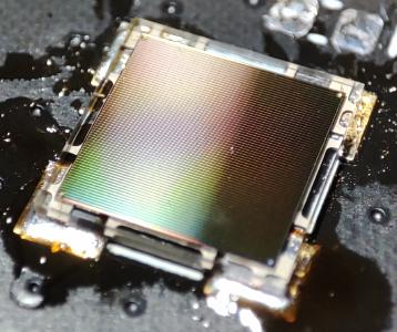
Silicon Photomultipliers (SiPMs) are Photomultipliers that make use the avalanche effect to multiply charge carriers generated by the photoelectric effect. It’s basically a parallel connection of thousands Single-photon Avalanche Diodes (SPADs). The key advantage if SiPMs over traditional photmultiplier tubes is that they are much smaller in space and do not need that much overvoltage. But, as always, they bring some disadvantages with them. This article gives a good knowledge about SiPMs.
Scintillation Detection Unit
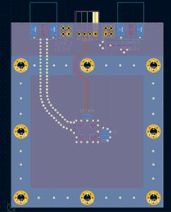
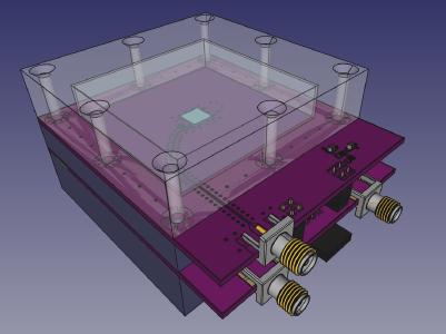
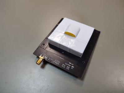
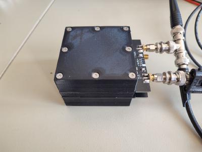
In order to properly model and design a charge measurement for a szintillation detector I had to model the combination of a BC-408 scintillator and a MicroFC-60035 SiPM first. I found this article explaining the fundamentals of silicon photmultipliers and giving an equivalent electrical circuit on which i based my simulation. BC-408 scintillator As always, the design process takes some iterations to come up with something one is satisfied with. The pictures below are showing a stack of to detection units, which could be used to determine whether and event happened in coincidence. This is useful to distinguish between events triggered by thermally generated free electrons inside the SiPM or by high energy particles instead.
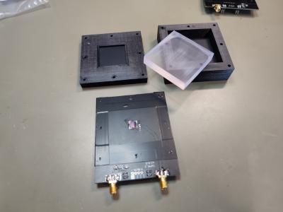
I decided to wrap the scintillator in aluminum foil as it has a pretty decent reflectivity for photons with a wavelength of $430~nm$. This is the wavelength which most of the photons that are emitted by the scintillator do have.
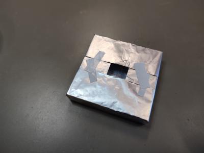

To protect the aluminum foile from mechanical stress, it’s additionally wrapped into tape. And a small peace of sponge is used to optain a better fitting of the sctintillator on top of the SiPM.
SIPM Spice Model
The following schematic shows the basic model of a SiPM used in the spice simulations. It consists out of active and passive SPADs as well as a parasitic capacity in parallel connection. In order for the simulation to work, one has to determine some parameters. But how does one do this? To get a good understanding i would suggest reading the article mentioned above.
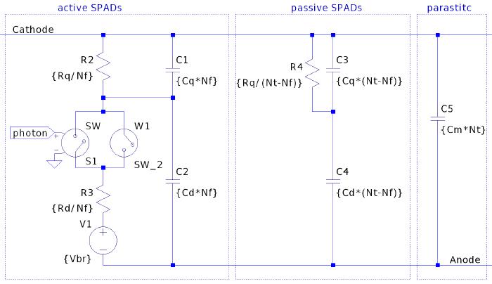
A Photon that triggers a avalanche break through is simulated by a voltage driven switch which is closed for a very short time in the single digit picoseconds range. As long as as the current through the other switch, which is current driven, does not get lower than $I_{th}$, it will stay closed. $I_{th}$ is the current down to which an avalanche break through can be self sustainable.
$$ \begin{equation} I_{th} = \frac{V_{Overvoltage}}{R_d + R_q} \end{equation} $$
$R_d$ and $R_q$ are related to the time constants of the rising and falling edges of the pulses.
$$ \begin{eqnarray} T_{fall} &=& R_q \cdot (C_d + C_q) \newline T_{rise} &=& \frac{R_d \cdot R_q}{R_d + R_q} \cdot (C_d + C_q) \newline a &=&\frac{T_{rise}}{C_d + C_q} \newline \Rightarrow R_d &=& \frac{a \cdot R_q}{R_q - a} \end{eqnarray} $$
$$ \begin{eqnarray} \end{eqnarray} $$
The total capacity of a single SPAD $C_{M}$ could in my case be calculated using the datasheet.
The article mentioned above tells us that $C_q$ and $C_d$ are linked to the gain $G$ and overvoltage $V_O$ of the SiPM, what somehow makes sense as the SPADs are reverse biased.
An increasing reverse bias voltage has to also increase the depletion region, which would result in a lower capacitance of the p-n-junction.
$$ \begin{eqnarray} G &=& V_{Overvoltage} \cdot \frac{C_q + C_d}{q} \newline \Leftrightarrow C_q + C_d &=& \frac{G \cdot q}{V_{Overvoltage}} \newline \end{eqnarray} $$
$C_S$ is the total capacity of the SiPM between anode and cathode, $N_t$ the total amount of microcells (SPADs) in the SiPM and $C_m$ the parasitic capactiy of a signel microcell.
$$ \begin{eqnarray} C^{’}_{M} &=& \frac{C_S}{N_t} \newline C_M &=& \frac{C_q \cdot C_d}{C_q + C_d} = C^{’}_M - C_m \newline \Rightarrow C_m &=& C^{’}_M - \frac{C_q \cdot C_d}{C_q + C_d} \end{eqnarray} $$
The table below shows the final parameters i came up with.
| Parameter | Value |
|---|---|
| $Cd$ | $97.3~fF$ |
| $Cm$ | $131.1~fF$ |
| $Cq$ | $95~fF$ |
| $Nt$ | $18980$ |
| $Nf$ | $[0, 18979]$ |
| $Rd$ | $2507~k\Omega$ |
| $Rq$ | $1165366~k\Omega$ |
| $Vbr$ | $24.45~V$ |
| $Vov$ | $2.5~V$ |
At this point it is important to mention that these parameters are measured/calculated for the complete detection unit.
They are not necessarily representing the SiPM’s parameters.
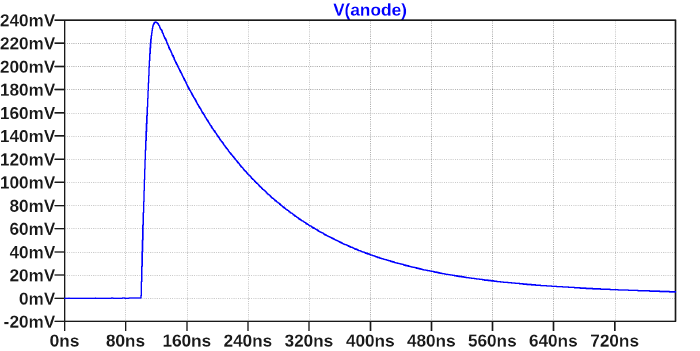
The picture below shows a simulation result with $3468$ firing microcells.